Wednesday, November 26, 2014

New Firmware for the IR Trigger

Some days ago I posted an article about a RC-1 clone infrared remote trigger for Canon SLR cameras. You can find it in this link.

The design included a quick and dirty firmware developed using Energia, an Arduino like environment for the MPS430 MCUs. This firmware was enough for testing most of the hardware but it could be improved. Mainly:

  • It didn't used the 32768 Hz watch crystal
  • It didn't used the resistors included to measure the battery voltage
  • It consumed 3.2mA in idle state so it was not efficient at all
Before talking about the code I should comment that there were a pair of errors in the schematic of the previous article. There are two changes that are indicated in blue in the following figure: The 22k resistors to measure the battery voltage were at incorrect pins. When soldering the components I changed the pins on the fly to ease the connections and I forget to update the schematic. In the same way the resistor and IR LED diode are swapped to ease, also, the connections.

IR Trigger Schematic v1.4

GCC Firmware

The new firmware was developed on the Portable MSP320 Environment I set up some days ago. The Texas Instruments sponsored Red Hat MSP430 GCC I used is a mixed bag. On one hand it provides an easy setup and an up to date selection of MCUs but on the other hand is not fully compatible with previous MSP430 code I developed for the MSP430 GCC at Sourceforge

The firmware code is distributed in three files:

This file includes some macros to ease the acces to bit fields on the MCU hardware registers.
I developed this file long time ago but I needed to do some modifications for this project due to the change of toolchain. Due to that, it is not guaranteed that all this file works in a particular toolchain.


This is the main file for the firmware. It practically contains all the code. It also includes some test code not used in the final firmware but that was left  behind.


This is the makefile that coordinates the build of all the firmware.


The code starts stopping the Watchdog and configuring the I/O ports. In particular it is very important to leave guarantee than there is no I/O floating as they will ruin the low power figures. In order to tie the unused lines to GND, the pull-downs are enabled on these lines.

Next, the 32768 Hz ACLK clock is configured and set as SMCLK. Then the main DCO clock is configured to operate at 16MHz using the Flash stored factory calibrated values.

After that, the push buttons SW1 and SW2 are configured to generate an interrupt when pressed. The configuration ends with the Timer0A that is connected to the 32768 Hz ACLK as input and associated with a capture interrupt RSI.

At the end of the initialization the red LED gives two blinks to indicate that the system is ready to operate.

After the initialization there is an infinite event loop. There are two possible events, each one associated to a function. If there is no event to process, the system enters in deep sleep LPM4 mode.

The Port 1 RSI associated to the pushbuttons generates the two possible events and gets out of LPM4 mode if needed so that the main event loop can process them.

As it was indicated there are two kinds of events. The SW1 button generates Normal Trigger Events that sends through the IR LED the signal that makes the camera shoot immediately. The SW2 button generates the Delayed Trigger Event that sends a similar signal that makes the camera shoot with a 2 seconds delay.

The signals associated to each event are composed on two 32768 Hz 16 cycles square wave bursts separated with some delay. That delay is used by the camera to identify both signals. The Normal Trigger signal has both bursts starts separated 7.82ms whereas the Delayed Trigger signal uses a 5.86ms separation.

The signals associated to those events are generated with an state machine associated to the Timer. An ISR execution associated to the Capture channel 0 of the Timer 0 provides the change from one state to the following one. The entry point to the state machine for the Normal Trigger Event is the Normal First Burst (NFB) state that connects the ACLK to the P1.4 pin during 16 cycles. After the state times out, the following Normal Delay (ND) state waits during 240 clock cycles. Then the Second Burst (SB) state outputs the second burst of 16 clock cycles to the IR LED. That ends the state machine for the Normal Trigger.
There is a sencod path in the state machine for the Delayed Trigger signal that starts with the Delayed First Burst (DFB) state. The only difference is this path is the second Delayed Delay (DD) state that is 176 cycles long instead of the 240 cycles associated to the ND state.
To provide some security against random errors, any undefined state goes to the NONE estate that stops the machine and also the associated timer.   

Timer State Machine

The use of an state machine is an efficient way to sequence the operations associated to the generation of the IR signal. At the start of the first state NFB, the SMCLK clock is sent to the P1.4 pin, the Compare register TACCR0 is set to 16 cycles in the future and the timer counter TAR is started in countinuous up mode.

Timer 0 TAR evolution and States
When the TAR counter reaches the TACCR0 value, an interrupt is generated. That changes the state from NFB to ND. The P1.4 pin is disconnected from the SMCLK clock and the TACCR0 Compare register is set 176 cycles in the future. When TAR reaches the 256 cycle mark a new interrupt is generated giving start to the SB state. A new burst is generated and TACCR0 is set 16 cycles in the future. Finally, at the 272 cycle mark, we enter in the NONE state where the burst ends and the TAR timer counter is stopped. 


Measurements

I have made some measurements to test the operation of the system. The following image shows the voltage at the IR LED diode during the first burst. We can see that there are 16 pulses.

Burst signal at the IR LED

To measure the clock frequency we can zoom in the burst pulses at the LED. We can see from it that the period is 30.6us so that the frequency is about 32680 Hz. As the start of the signal is not synchronized with the clock, the first pulse is not equal to the rest. In practice this is not a problem but, if it were, we could add another state in the machine to synchronize the burst start.

Burst pulse detail
The following figure shows the IR LED voltage for the full signal in normal non delayed camera trigger mode. We can measure a 7.81ms delay time between the start of both bursts. This is just the desired value.

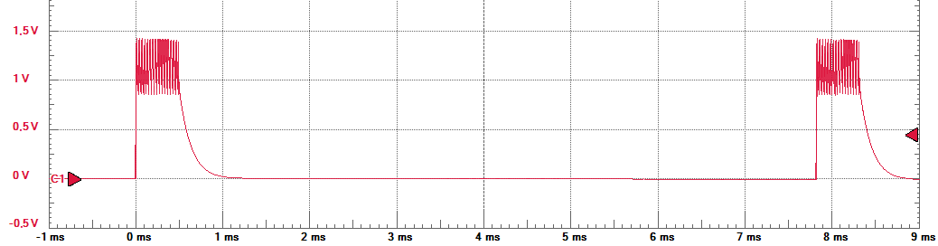
Normal Trigger Full signal
In the same way we can see that the delayed mode trigger features a 5.86 ms time between the start of the two bursts. So everything is ok.

Delayed Trigger Full signal
The above signals indicate that the IR LED has a non zero offset voltage. This is true but it doesn't affect its current. As the IR LED is a diode, it features an exponential relationship between its voltage and its current so by the time its voltage falls below 1V  the current is practically zero.

To test the real current on the diode we can measure the voltage on the current limiting 6.8Ohm resistor that is in series with the LED. We can see that the peak pulse voltage goes from 560mV at the start of the burst to about 470mV at its end. That means that the peak current goes from 82mA to 69mA. We planned for 100mA current and we could lower the current limiting resistor to increase the current, but in the end the CR2032 battery that powers the system could produce system resets due to the fall in the supply during the bursts.


Voltage at 6.8 Ohm resistor


Idle current

One of the most important drawbacks in the Energia firmware was the 3.2mA idle current. Using the GCC firmware we can use the low power LPM4 mode to significantly reduce this current.
From the information provided on the MSP430G2553 we know that the LPM4 current can be as low as 0.1uA.

Low Power figures in the MSP430G2553
Going to currents as low as that is not easy. 0.1uA at 3V means an equivalent resitance of 30 MOhm. Just touching the battery terminals will give a much greater current. That means that we must take care that no current in wasted during the sleep time. As we have commented, all unused pins are tied down to GND using the integrated pull-down resistors. That includes the port 3 lines that are not used in the DIP20 package.
Using this method I obtained in practice the datasheet indicated value of 0.1uA for the typical scenario at 25ºC as you can see in the image below. 0.1uA  is so low that we don't need to power down the circuit at all as the battery will live ages with that current.

0.1uA current at LPM4 mode

Power supply measurement

The firmware also includes a measurement of the power supply after each signal sent. The ADC uses the 1.5V internal reference because the 2.5V one cannot be used below 2.8V. That means that our resistor divider used to measure the supply will get just the maximum 1023 10 bit count at 3V. The system detects the low voltage condition when the voltage falls below 2.6V, that means that the voltage at the divider is 1.3V so that the ADC gives about 890 counts.

The firmware lights the red LED during 400ms after each transmited signal. When it detects a low battery voltage condition the LED is not turned on so that the user can see that the battery is nearly depleted.


Last words


That's all for now. The code currently ocupies about 2500 bytes with no optimization and with debug enabled. Disabling the debug and turning on the compiler optimizations its size falles to about 2000 bytes. That leaves a lot of room for future firmwares improvements as the MSP430G2553 features 16KB of flash memory.
In fact, the project could be developed in a smaller MCU but given the price differences in the MSP3250G budget line at low volumes there is little to gain in costs selecting another MCU.


Gist Update (30/11/2014)

Thanks to Gist, now the code, with syntax highlighting, is now included inside the blog entry.

Code on Github (11/02/2018)

This new firmware and the old energia one are now on Github:

https://github.com/R6500/Canon-IR-trigger


Sunday, November 23, 2014

LED Light Teardown

Today I have made a tear down and reverse engineering of a cheap 12V LED light that is designed to substitute a 12V halogen lamp. Let's see what it is inside.

12V LED Light
The LED light is composed of 21 small white LEDs. The package says it's 1W. Applying 12V we I get 87mA so it is trully 1W. But what efficiency we get on the circuit?


The insides

After breaking the enclosure we get the lamp internals.

Lamp internals
The lamp is internally composed on two boards. One round board holds the 21 LEDs and a smaller octagonal board holds the control circuit.

LED Board


The LED board is painted white at the LED side to give a better reflectance of stray light.
Before continuing the tear down, I liked to check the curren on one of the LEDs. To do that, I disordered a LED and re soldered only one terminal to put a multimeter in series.

Current meas setup
Measuring the LED current when operating it gives 10.5mA. Those are quite simple LEDs. More modern LED lamps use high current devices. That's why it needs 21 LEDs to get 1W of power.

Continuing the tear down, I have separated the two boards and removed all LEDs from the led board. The front side has markings so we can see where should be the anode and cathode of each led.

LED board: Front

The back of the led board holds all the connections. From them we can see that the 21 LEDs are arranged in seven parallel groups of 3 LEDs in series. As one white LED can have a forward current of up to 3.5V, we cannot use more than three LEDs in series if we use a linear control circuit. We also don't want to put less than three LEDs because that will give less efficiency.


LED board: Back
As a result of the tear down we get also a bunch of leds.


Bunch of LEDs


Reverse engineering of the circuit

The circuit used to power the LEDs is shown in the next figure.

Control Circuit
There are two input cables for the AC 12V input source and two output nodes (+)  and (-) to connect the seven stripes of three LEDs.
To get the circuit schematic I have taken a photo of the back of the board. I have mirrored it to have the same positions as the component side and I have written down all the components present on the board.

Component distribution on the board


The equivalent schematic of the board follows:

Circuit schematic
Nothing fancy. Just a linear current control regulator.
The four diodes take the 12V AC input source and rectify it to get, with the help of the capacitor E1, a constant voltage between Vdd and GND. 
The diodes have a marking RS1M. Those seems to be standard 1A silicon diodes. The voltage at 87mA should be around 0.7V. As we have two voltage drops, that gives a Vdd-Vss voltage of about 10.6V.
The LEDs are connected to the collector of the big transistor Q1 (D882). The base current of Q1 is fed by the resistor R2. 
The base of Q1 is at two Vbe drops over Vss, so, about 1.2V. That gives a maximum base current of  3.1mA. That means that we can drive the 87mA current of the 21 LEDs with a minimum forward beta (current gain) of  28.
We need, of course a way to limit the current at the LEDs. That's the mission of Q2.
The collector current in Q1 is similar to the emitter current that goes to R1. As the base-emitter junction of Q2 is connected to this resistor, when it reaches about 0.6V, Q2 will turn on and drain the base current of Q1. The equilibrium point of the circuit is where Q2 is just starting to turn on and the current at Q1 will be at about 0.6V/R1 that gives 80mA. This theoretical result is quite similar to the measured current of 87mA.

I have measured one of the LEDs and it gives about 3V at 10mA. For a series of three LEDs we get 9V. The voltage at R1 is 0.6V. That gives a voltage drop of about 10.6V - 9V - 0.6V = 1V between the collector and emitter of Q1. Enough room for voltage drop changes on the diodes as function of the temperature.

If we consider that we get a total voltage of 9V on the LED strips from a source voltage of 12V, that means that the circuit efficiency cannot be better than 75%. It could be better using a DC/DC voltage to current converter instead of using linear circuit but what can you expect from a 3€ LED lamp?

Tuesday, November 18, 2014

Portable environment for the MSP430 Launchpad


I love portable environments. I like programming using an external hard drive, moving the HDD from one PC to another, and continue programming using the same tools and data.

Here I explain the method I use to create a Windows portable Eclipse based development environment for the MSP340 family using the Launchpad as the programming/debugging link.

MSP430 Launchpad

As a compiler I will use MSP430 GCC. For every element in the toolchain I try to use as much open software tools as possible but I will also try to keep things simple so sometimes it will be a compromise.

This is a deep rewrite of the portable development environment for the MSP430 Launchpad board  I set up in 2012. I then wrote an article in my spanish blog AIM 65 and, since then, some things have changed. So, here I am repeating all the steps I made before. Some things are the same but most are quite different.

This procedure works in Windows 7 and it should work also in Windows XP. Don't know about other operating systems.

Basics


Unfortunately Eclipse is not fully portable between machines. Some paths in the projects are absolute, not relative. That means that if you want to move your Eclipse development environment from one machine to another you have to guarantee that the files have the same location in both places. The easiest way to do that is changing the drive letter in windows so that it is the same in any machine. In my case, my moving HDD uses the letter M, so its M: on all systems.

Check your operating system for the method to assign the external drive letters. It usually involves using the Disk Manager, selecting the drive and selecting one option with the right mouse button contextual menu.

Eclipse is a java application. That means that you need to have java installed in any computer where you want to use the development environment.

There are several free toolchains available for the MSP430 devices. Texas Instruments provide a free version of the Code Composer Studio. As they state:

"A free license will be generated that supports a 16KB code size limit for the optimized TI compiler or no code size limit with GCC."

You are limited to 16KB but as no MSP4340 value line MCU has more memory that that it's no big deal. Moreover, you can always USE GCC and not be constrained at all.

If you want to have an easy install of the tools needed to develop on the MSP430 value line of MCUs, nothing is easier that downloading and installing CCS.

This application is not, however, the target of this article.

One of the complex elements in the development environment is the debug chain. To successfully debug successfully a MSP430 device you usually need:

  •     USB drivers for the board of FET used
  •     DLLs needed to communicate with the USB drivers
  •     GDB Proxy to communicate with a GDB program
  •     GDB program

The GDB program is usually included with the compiler but the rest of the elements sometimes have to be found in different places.

Fortunately nowadays the USB drivers are detected and installed automatically and Texas Instruments provides a file that provides the rest of elements together with the GCC compiler.


Downloading the files


First, we will start downloading the required files.

Go to  the Eclipse donwload web page http://www.eclipse.org/downloads/ and download the required installer. At the time of writing this article it was Eclipse Luna.

Eclipse Luna Download
As I'm using Win7 32 bit I selected the 32 bit installer.

Then we need to download the make and other Unix-like companion commands from this link:


You should get a UnxUtils.zip file.

Finally you should get the Red Hat msp430 gcc compiler from Texas Instruments using this link:


MSP430 GCC at Texas Instruments

You could use the MSPGCC from the sourceforge location. The problem is that it doesn't include all the needed debug elements.

Second Step downloading MSP430 GCC

That will lead to a page were you need to use a TI account to download the software. It's free, but it could not suit everyone.
At the end you should get a file with a name like msp430-gcc-full-windows-installer-2.1.1.0.exe.

That are all the files needed to download. You should have something like this list:

  • eclipse-cpp-luna-SR1-win32.zip
  • UnxUtils.zip
  • msp430-gcc-full-windows-installer-2.1.1.0.exe

Creating and filling the directories

I locate all the microcontroller files inside a MCU folder insider M:. You can  do as you please but you'll need to change the directories.

Create the main directory, in my case, as I use Eclipse Luna it will be:

M:\MCU\msp430_Luna

Open the eclipse zip file and copy the eclise folder it contains over the newly created directory.
The main executable of all the environment will be M:\MCU\msp430_Luna\eclipse\eclipse.exe. Feel free to put a link to this file somewhere that is easy to reach like your desktop or your main folder in the external drive.

Create te following four directories inside M:\MCU\msp430_Luna:

  • UnxUtils
  • msp430-gcc
  • workspace
  • projects
Copy the contents of UnxUtils.zip inside the UnxItils directory.
Finally execute the msp430-gcc-full-windows-installer-2.1.1.0.exe GCC installer, accept the license and instruct it to put all the files inside the msp430-gcc folder.


MSP430 GCC Install
 So far we have filled the eclipse, UnxUtils and msp430-gcc folders and we have empty the workspace and projects folders.


Configuring Eclipse


Now it's time to run and configure eclipse. Run the eclipse.exe program located inside M:\MCU\msp430_Luna\eclipse (directly or using a previously created link).
You will see a window like the one shown that prompts for a workspace folder.

Eclipse workspace selection
Select M:\MCU\msp430_Luna\workspace and hit OK.

After some initialization you will see a window like that:

Eclipse Start Window
Before continuing we must install the needed debug elements inside eclipse. To do that, select "Install New Software" from the Help menu.

Install new software
Select "All Available Sites" as "Work with" option and write down "GDB Hardware Debugging" as is shown in the next window. It can take a while to do the search.

GDB Support Installation
Select the C/C++ GDB Hardware Debugging item and click Next.
Hit Next in the following window, accept the License in the next one and click Finish.

After the install it will prompt to restart, let it do it and use the same workspace when it restarts.

Restarting Eclipse
You will get the same start screen. Here click over the workbench icon to continue.

Workbench ICON
That will give the standard Eclipse C/C++ view:

Eclipse C/C++ view


Compiling a Blink example

Next step is to compile a simple example. In embedded systems a LED blink program is the equivalent of a hello world program in a normal console C program.
The msp430 GCC distribution comes with an example.
I don't like to compile the program in its provided location, so I suggest to copy it to the projects folder, that means copying the folder:

M:\MCU\msp430_Luna\msp430-gcc\examples\windows\msp430g2553

To the projects folder location:

M:\MCU\msp430_Luna\projects

And rename it from msp430g2553 to blink

That way you should have the following folder contents:

Blink project contents
Then we will include this project in Eclipse using the New "Makefile Project with Existing Code" option inside the File menu.

Creation of a Makefile Project

That will give a dialog window were you can use the browse button to locate the project directory. Eclipse will give it the "blink" name. You can leave as is or change it.

Creation of new project dialog
After clicking on "Finish" the project will be created and you return to the C/C++ view.
Then, you can use the project explorer to view the contents of the Makefile.

Original project Makefile
As we have moved the make file from its original location we need to change the paths.
You can use relative or absolute paths, using relative paths you can set:

GCC_DIR =  ../../msp430-gcc/bin
SUPPORT_FILE_DIRECTORY = $(GCC_DIR)/../include

Then we can change the -O2 optimization option to -O0 so that the compiler doesn't optimize the code. This is needed if we want to do step by step debugging as the compiler optimizations break the relation between written and executed code. After all debugging is done its best to replace -O0 with -O2 to optimize the program so that the memory is reduced and the program speed is increased.

Finally, we can change the name of the output file to do that, we will create a new variable called "EXECUTABLE" and use it in the GCC reference.
As we won't use the GDC target in the makefile and we could era its last two lines.
That will give the following Makefile.
Makefile modifications
This is the final Makefile after all modifications:


Observe that the makefile is designed to use a MSP430G2553 MCU, this is the MCU mounted on the MSP430 Launchpad version 1.5 board. If you want to compile for another MCU you should change this line.

After all modifications are made you can save them using the save button.
You can also examine the main blink.c source file:

blink.c source file
 You will see that there are plenty of errors. As this is not an eclipse managed project, the error checker don't know how to process the includes needed to provide several literal definitions. As those errors are quite ugly we can remove them. To do that, select the Project properties on the contextual menu on the blink folder of the Project Explorer. And then select Code Analysis and unselect the 5 elements than end in "..resolved". Then hit OK.

Code Analysis
That will get us rid of those nasty error messages.
 
The last step to obtain an executable is to compile the project. Just select Build Project in the Project menu.

Building the project
 If all goes well you will see something like that in the console:

Console after compilation
You can now see in the project explorer that you have two new files in the blink directory . The blink.o object file obtained from the compilation of blink.c and the blink (with no extension) executable file.

Optionally we can create a command to see the memory usage of the program.
To do that, select External tools configuration in the contextual menu in the tools icon.

External tools
Select program and click the New Launch Configuration button. And fill the data indicated below:

Name: Resource Size
Location: M:/MCU/msp430_Luna/msp430-gcc/bin/msp430-elf-size.exe
Working Directory: ${container_loc}
Arguments: ${resource_loc}

Resource size main tab
In the build tab unselect Build before launch.

In the Common tab select External Tools in the Display in favorites menu section.

After that, just hit Apply and then Close.

To see, for instance, the size of the executable binary file we can select it in the Project explorer and select the Resource Size element in the External tools menu.

Resource size of the main binary file
Here we can see that the binary file includes 708 bytes of code for a total size of 746 bytes. As the MSP430G2553 features 16KB of flash memory we have plenty of space left.


Program Run and Debug

To program and run the program on the MSP430G2553 MCU included in the Launchpad board we need o use several software elements.

First we need the USB drivers for the launchpad board. They will normally be installed automatically when you connect the board to the computer, but if you need to manually locate them, there are some drivers in this location inside the GCC folder:

M:\MCU\msp430_Luna\msp430-gcc\emulation\drivers\msp430

Alternatively you can download the energia drivers from:


Then we need to start the GDB Agent that will communicate the gdb program with the USB drivers. I was not able to properly use the command line program gdb_agent_console.exe without debugging errors so I used the GUI version gdb_agent_gui.exe file instead.
You can run this program directly but I prefer to run it from eclipse. To do that you can create a new external tool configuration:

Name: GDB Agent GUI
Main TAB:
  Location: M:\MCU\msp430_Luna\msp430-gcc\bin\gdb_agent_gui.exe
  Working Directory: M:\MCU\msp430_Luna\msp430-gcc
Common TAB:
  Select tick in External Tools

Then click Apply and then close. You have now the GDB Agent GUI program next to the Resource Size one. Launch the GDB Agent GUI and then click on Configure and select msp430.dat. After that click on the Start button.
If all goes well you will see a "Waiting for client" message like in the following window:

GDB Agent
After the GDB agent is successfully running we need to create a debug configuration. Use the contextual menu on the debug icon to select Debug Configurations...

Select Debug Configurations
Selecting GDB Hardware Debugging, click on the New Launch Configuration button and fill the following data:

Name: Blink
Main TAB:
  C/C++ Application: blink
  Project: blink (Select it from the browse button)

Debug configuration Main tab
Then click on Select other... at the bottom of the window and select in the new window Use configuration specific settings and Legacy GDB Hardware Debugging Launcher. Then click OK.

Selecting the debugger launcher

Next continue with the other tabs:

Debugger TAB:
  GDB Command: M:\MCU\msp430_Luna\msp430-gcc\bin\msp430-elf-gdb.exe
  Port number: 55000


Debugger tab

Startup TAB:
  Set breakpoint at: main
  Resume

Startup tab

Common TAB:
  Set tick in Display in favorites menu "Debug"

After that, Apply all changes and then Close.

Now you have a new element in the debug icon contextual menu. Check that the GDB Agent is still running and select the Blink option in the debug icon contextual menu.

Launch the debugger
You will see message recommending to change the perspective to the debug one. Just say yes.


The Debug View will open and you will see something like the following window.

Debug View
We see that the program is stopped at the start of the main program. To continue running the program just push the play button.

You should see the red LED blinking on the Launchpad board. Congratulations!!!

You can now use the pause button to pause program execution. To continue, just push the play button another time. You can also see the variables contents and use breakpoints but all that goes out of the scope of this long article.

To end the debugging you can hit the Terminate red square icon and remove the terminate debugin session selecting it and hitting the DEL key.

Terminate the debugging session
After all debug is done, the GDB Agent can also be terminated selecting it and pushing the red square terminate button. After that, the DEL key will eliminate it from the debug view.

Closing Words

After all this work we have a blink project and a MSP430 portable development environment to be used with it. To create a new project you can duplicate the blink entry on the projects folder and repeat the needed steps to incorporate the project in eclipse.

You don't need to repeat the creation of the items in the run programs menu, but you must replicate the debug entry for each new project. To do that, the easiest way is have the blink and the new projects open at the same time and duplicate the debug entry in the debug configurations window.

Duplicating a debug configuration
That's all for now. The eclipse environment is so complex that there is no more space in this article to talk about it. I will probably write more on the subject in future articles.


Compiler woes   (update at  November, 25  2014)

It seems that the TI sponsored msp430 gcc compiler is not able to determine how to do multiplications on the MSP430G2553. I got strange results in multiplications and I suspect that the compiler is trying to use a hardware multiplier that this MCU lacks.

I needed to do some guesswork to find the needed  -mhwmult compiler option as I could not find where it is documented. Finally I know, by asking the gcc compiler, that there are 5 available options: 16bit, 32bit, auto, f5series and none.

In order to correctly compile the code I had to include the compiler option:

 -mhwmult=none

That way multiplications go as they should.

The interrup macro at iomacros.h is also broken. It is defined:

#define __interrupt(vec) __attribute__((__interrupt__(vec)))

but msp430-gcc don't like this format. I have developed a new definition:

#define interruptNew(vec) __attribute__((interrupt(vec)))

That way I can properly compile, for instance, the port 1 RSI:

void interruptNew(PORT1_VECTOR) PORT1_ISR (void)
 {

 // Do RSI things
 }


Gist Embedded Makefile (Update at 30/11/2014)

Now the Makefile code is embedded in the blog using Gist